click on picture to see larger image
| NOTE: 'N5FC' is my former call. This project was constructed while that call was valid, and you may observe references to it. |
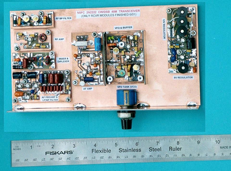
| Progress! | I'm finally cutting boards and making progress on this project, which as of July 2001 is about 2/3 complete. The receiver is functional, but I'm adding AGC, and the VFO needs a little work (or else I'll just call it "The Driftmaster"). The transmitter has not been started yet, but it's gradually floating to the top of my list. Keep checking back! |
| Sorry! Under Construction! | but here's what we have so far... |
In spring of 1998, NorCal sponsored a contest to design and build a project using no ICs and 22 or fewer 2N2222s as the active semiconductor devices. I thought this was a really intriguing idea, so I set about to design my version. Unfortunately, I only got as far as the paper design and buying parts before the Dayton Ham Convention came and went. [the winning project, by K8IQY, can be seen -here-]
I still intend to assemble my version, but in the meantime, you're welcome to get started without me. I'll list the schematic for download at the end of this narratives, along with any other pertinant data I have. My version is a 40 Meter CW/DSB (Double-Side-Band) Transeciver. It uses 22 each 2N2222's and will run from 12 Volts. The Receiver is a direct-conversion design with a switchable input attenuator and RF preamp, diode balanced mixer (diodes were allowed), a switchable low-pass-band-pass passive filter, and audio amplifier. (I may replace the audio final with the version presented by K8IQY, which I like much better). The Local Oscillator also serves as the VFO during transmit. The oscillator is a Colpitts design with varactor tuning, and two-stage buffer. Tuning is provided by two front-panel pots, Main and Bandspread, and an offset is provided during transmit.
During transmit, the VFO is routed through a tuned pre-driver and tuned driver stage (both class A), and then to the class AB push-pull linear final amplifier. The final should develop about 1.5 watts pep. A 5-element Pi-type low-pass filter is used to reduce harmonics before being coupled to the antenna. A top-hat type heat sink is used on each of the final transistors, and thermal coupling is provided to the final's bias supply. Mic audio (in DSB mode) is first routed through a 2.75 KHz passive LC lowpass filter, then through a high-gain audio stage, to the diode-type balanced modulator. There is no ALC circuit to prevent overmodulation or splattering (A diode clipper might be in order). Keying circuits route the VFO output from receiver to transmitter, and key the RF driver stages. SPICE simulations indicate the backwave is suppressed by 82 dB, but I'll believe that when I see it.
Although the contest rules would have allowed external regulated power supplies, I decided to accomplish all regulated voltages using regulators built from 2N2222s. The first regulator, outputing 12 Volts and current limited at 0.4 A, is routed to all stages. Heat sinks are required. A secondary regulator, at 8 Volts output, provides a stabilized supply for the VFO and tuning varactor. An external unregulated DC supply should supply 15-17 volts (a wall transformer might be a suitable candidate).
I did SPICE simulations on critical circuits, for verification and tweaking purposes. On the VFO, the output level (at Q9 out) was confirmed to be reasonably sinusoidal at 5mW into a 100 ohm load. RF drivers were confirmed as providing enough gain to supply about a quarter watt to the finals (way more than enough to drive the Class AB linear final). The 12 Volt regulator circuit showed 120 Hz ripple to be down 47 dB (input/output), and an additional 25 dB down at the output of the 8 Volt regulator. Startup and shutdown is smooth through the regulators, with no overshoot. No-load to full load (0.25A) regulation is &3% (12.49 to 12.16V nom) for the 12 Volt regulator. Keying of the RF stages shows a smooth risetime and decay time of about 0.2mS (which may be a little harsh), with no overshoot. Backwave in the RF stages simulated to be down 87 dB, which is an excellent figure, but a little hard to believe for bipolar keying circuits. I confirmed gain and minimal distortion (&10%) through the audio stages of the receiver and mic circuits. I also confirmed frequency response for the passive audio filters (you can view plots below).
I intend to assemble all of this into an aluminum chassis (LMB 5942), approximately 9.5 x 5 x 2 inches. Hopefully, I'll get started one of these days. Hopefully, it will work ;-)
Unfortunately, the only schematics I have available are in MS Word format, or a .jpeg file, both fairly large. In order to pick up the detail (in the drawings), I scanned at fairly high resolutions, then converted to .jpeg files. You can view them on your monitor if you have a fairly high-res model, but most will want to print them from a graphics viewer. Usually, this can be done by right-clicking on the open image, then saving it as a file in a directory/folder of your choosing, and then opening it with your graphics viewing software. HTML browsers (like Internet Explorer and Netscape) are terrible at printing large graphics files, and refuse to scale them under user control, but the graphics editing programs do a good job of it. In your editor's options, select to scale to page size (usually in landscape orientation).